CMOS Imaging Principle:What is the fundamental principle behind CMOS imaging?
Q: What is the fundamental principle behind CMOS imaging?
A: The CMOS imaging principle is based on converting light into electrical charge using a photodiode within each pixel. When photons strike the silicon photodiode, they generate electron-hole pairs via the photoelectric effect. The electrons are collected in a potential well, and the accumulated charge is proportional to the light intensity. Unlike CCDs, each CMOS pixel contains its own amplifier and readout circuitry, allowing parallel readout of all pixels. The charge is converted to a voltage by a floating diffusion node, then amplified and digitized. This in-pixel amplification reduces power consumption and enables high-speed operation, making CMOS sensors dominant in modern cameras. Key steps include photon absorption, charge generation, charge-to-voltage conversion, and signal readout.
Q: How does a CMOS sensor differ from a CCD sensor in terms of working principle?
A: The CMOS imaging principle differs from CCD in charge transfer and readout. In CCD, charge packets are shifted sequentially across the chip to a common output amplifier, requiring high voltages and specialized fabrication. CMOS sensors use a passive or active pixel architecture where each pixel has its own transistor amplifier. The charge is converted to voltage directly at the pixel, and readout is performed row by row via column wires. This eliminates the need for charge transfer, lowering power consumption and enabling on-chip integration of timing, control, and analog-to-digital conversion. CMOS also supports random access to pixels, which is beneficial for region-of-interest readout. However, CMOS pixels may suffer from higher fixed-pattern noise and lower fill factor due to in-pixel transistors, though modern designs mitigate these issues.
Q: What are the main noise sources in CMOS imaging and how are they mitigated?
A: In CMOS imaging, major noise sources include photon shot noise, dark current, read noise, and fixed-pattern noise. Shot noise arises from the quantum nature of light and is unavoidable. Dark current is thermally generated charge, reduced by cooling or using pinned photodiodes. Read noise comes from the pixel amplifier and reset transistor, minimized by correlated double sampling (CDS) and low-noise circuit design. Fixed-pattern noise due to transistor mismatch is corrected by on-chip calibration or digital correction. Additionally, 1/f noise in amplifiers is addressed by chopping or larger transistor sizes. Modern CMOS sensors also employ buried photodiodes and transfer gates to reduce dark current and reset noise. Overall, noise mitigation combines process technology, circuit techniques, and digital post-processing to achieve high signal-to-noise ratios.
Q: How does the photodiode in a CMOS pixel convert light into an electrical signal?
A: In a CMOS pixel, the photodiode is typically a pinned diode formed by a p-n junction. When light enters the depletion region, photons with energy greater than the silicon bandgap (1.1 eV) excite electrons from the valence to the conduction band, creating electron-hole pairs. The built-in electric field separates the carriers: electrons accumulate in the n-type region, while holes flow to the p-type substrate. This accumulation reduces the depletion width and changes the junction capacitance. After exposure, a transfer gate moves the electrons to a floating diffusion node, where the charge is converted to a voltage via Q=CV. The voltage is then buffered by a source follower and read out. The linear relationship between photon flux and collected charge enables accurate light measurement, forming the basis of CMOS imaging.
Words of experience
Common scenarios of "CMOS Imaging Principle"
【Student】 Professor, I'm trying to understand how a CMOS image sensor works. Could you explain the basic principle?
【Professor】 Certainly! A CMOS image sensor converts light into electrical signals using an array of pixels, each containing a photodiode and several transistors.
【Student】 What does the photodiode do exactly?
【Professor】 The photodiode absorbs photons and generates electron-hole pairs, creating a charge proportional to the light intensity.
【Student】 How is that charge then read out?
【Professor】 Each pixel has a transfer gate that moves the charge to a floating diffusion node, which converts it to a voltage.
【Student】 And then that voltage is amplified?
【Professor】 Yes, a source follower transistor amplifies the voltage, and a row select transistor allows the pixel to be read out to the column bus.
【Student】 So each pixel has its own amplifier? That seems different from CCDs.
【Professor】 Exactly. In CMOS, each pixel has active transistors, enabling parallel readout and lower power consumption compared to CCDs.
【Student】 What about color? How does a CMOS sensor capture color?
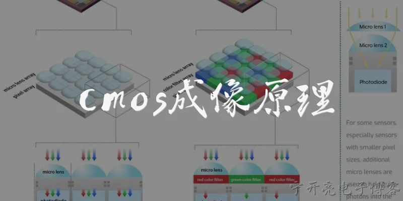
【Professor】 A color filter array, usually a Bayer pattern, is placed over the pixels, with each pixel sensitive to red, green, or blue light.
【Student】 Then demosaicing is used to reconstruct the full-color image?
【Professor】 Correct. The raw data from the Bayer pattern is interpolated to produce a full-color image for each pixel.
【Student】 What are some advantages of CMOS over CCD?
【Professor】 CMOS sensors are cheaper to manufacture, consume less power, and can integrate additional circuitry on-chip, like analog-to-digital converters.
【Student】 Are there any disadvantages?
【Professor】 Early CMOS sensors had higher noise and lower sensitivity, but modern designs have largely overcome these issues.
【Student】 How does the sensor handle exposure time?
【Professor】 Exposure is controlled by the reset and transfer signals; the time between reset and readout determines the integration period.
【Student】 That makes sense. Thanks for the clear explanation!
【Professor】 You're welcome! Feel free to ask if you have more questions.