Forward Converter Switching Power Supply Design:What is a forward converter and how does it work in a switching power supply?
Q: What is a forward converter and how does it work in a switching power supply?
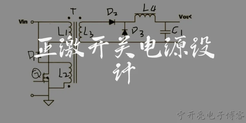
A: A forward converter is an isolated switching power supply topology that transfers energy to the output during the switch's on-time. When the primary switch turns on, current flows through the transformer primary, inducing a voltage on the secondary. A rectifier diode then conducts, and an inductor-capacitor filter smooths the output. Unlike flyback converters, which store energy in the transformer during on-time and release it during off-time, the forward converter transfers energy directly. To prevent transformer saturation, a reset winding or active clamp is used to demagnetize the core during off-time. The duty cycle is typically limited to below 50% to allow core reset. Forward converters are efficient for medium power levels (up to a few hundred watts) and provide good regulation with minimal output ripple, making them suitable for applications like telecom and industrial power supplies.
Q: What are the key design considerations for a forward converter transformer?
A: Designing the transformer for a forward converter involves several critical factors. First, select a core material and size based on power level and switching frequency; ferrite is common for high frequencies. The turns ratio must be chosen to achieve the desired output voltage from the minimum input voltage at maximum duty cycle. Core reset is essential: a reset winding with the same turns as the primary or an active clamp circuit ensures the flux returns to zero each cycle, preventing saturation. The magnetizing inductance should be high enough to limit magnetizing current but not so high that it slows reset. Leakage inductance must be minimized to reduce voltage spikes and losses; interleaving windings helps. Insulation between primary and secondary is crucial for safety. Thermal management is also important, as copper and core losses generate heat. Finally, verify that the transformer can handle the peak currents without saturation.
Q: How do you select the output filter components for a forward converter?
A: Selecting the output filter for a forward converter involves choosing the inductor and capacitor to meet ripple and transient requirements. The inductor value is determined by the desired ripple current, typically 20-40% of the maximum load current. Use the formula L = (Vout × (1 - D)) / (ΔIL × fsw), where D is duty cycle and fsw is switching frequency. A larger inductor reduces ripple but increases size and cost. The output capacitor must handle the ripple current and maintain voltage ripple within specifications. RMS ripple current in the capacitor is roughly ΔIL / √12. For low ESR, use multiple capacitors in parallel. Also consider the closed-loop stability: the output filter forms a double pole that affects the control loop. The crossover frequency should be well below the filter's resonant frequency. Finally, account for derating and thermal effects to ensure reliability over the operating temperature range.
Q: What are the common challenges in forward converter design and how to mitigate them?
A: Forward converter design faces several challenges. Transformer core reset is a major issue; without proper reset, the core saturates, causing excessive current and failure. Mitigate with a reset winding, active clamp, or resonant reset. Voltage spikes due to leakage inductance can damage the switch; use snubber circuits or clamp circuits to absorb energy. Duty cycle limitation (typically <50%) restricts the conversion ratio; for wide input voltage ranges, consider a different topology like flyback or use a tapped inductor. Cross-conduction in synchronous rectification can reduce efficiency; ensure proper dead time. EMI is another concern; use shielding, proper layout, and input filters. Thermal management is critical because of high currents and switching losses; use adequate heatsinking and airflow. Finally, loop compensation must be carefully designed to ensure stability across load and line variations. Each challenge requires trade-offs between cost, efficiency, and complexity.
Dialogue about
Common scenarios of "Forward Converter Switching Power Supply Design"
【Power Electronics Engineer】 Hi, I'm designing a forward converter switching power supply for a telecom application. I need some guidance on the initial specifications. Can you help?
【Senior Design Consultant】 Absolutely! I'd be happy to help. Let's start with the input and output requirements. What are your input voltage range, output voltage, and current?
【Power Electronics Engineer】 The input is a standard telecom DC bus, 48V nominal, ranging from 36V to 75V. Output is 12V at 20A, so 240W.
【Senior Design Consultant】 Got it. For a forward converter, you'll need a transformer for isolation and voltage step-down. Since input can be as low as 36V, the turns ratio should be chosen so that at minimum input, you can still regulate 12V. Let's calculate the required duty cycle at nominal 48V. Assuming a 0.5 max duty cycle, the secondary voltage should be at least 24V. So a turns ratio of 2:1 would give 24V at 48V input. But at 36V input, secondary is 18V, which is above 12V, so duty cycle can be adjusted. That seems reasonable.
【Power Electronics Engineer】 That makes sense. So primary to secondary turns ratio Np:Ns = 2:1. Now, what about the reset winding? I know forward converters need a reset mechanism to avoid core saturation.
【Senior Design Consultant】 Correct. The most common is a third winding with the same turns as the primary, connected to reset the core during off-time. Alternatively, you can use an active clamp or a resonant reset. For simplicity, let's use a reset winding with Np turns. During off-time, the magnetizing current flows through the reset winding and the diode back to the input, resetting the core. The maximum duty cycle is then limited to less than 0.5 to allow complete reset.
【Power Electronics Engineer】 Okay, so with a reset winding, the duty cycle must be less than 0.5. At minimum input of 36V, we need 12V output. With a 2:1 turns ratio, secondary voltage is 18V. To get 12V, duty cycle D = 12/18 = 0.667, which is greater than 0.5. That's a problem!
【Senior Design Consultant】 Good catch. So we need to adjust the turns ratio. We need D_max <= 0.45 for margin. At minimum input, V_secondary = V_in * (Ns/Np). We need V_secondary * D_max >= 12V. So V_secondary >= 12/0.45 = 26.67V. At 36V input, Ns/Np >= 26.67/36 = 0.74. So Np:Ns <= 1.35. Let's choose Np:Ns = 1:1, i.e., Ns = Np. Then at 36V input, secondary is 36V, D = 12/36 = 0.333, which is fine. At 75V input, D = 12/75 = 0.16. That works.
【Power Electronics Engineer】 So turns ratio 1:1. That means the transformer is not stepping down voltage, which is fine since we have duty cycle control. Now, what about the output inductor? I need to design it for continuous conduction mode.
【Senior Design Consultant】 Yes. The output inductor value depends on the ripple current. Let's target a ripple current of 20-30% of full load, say 6A peak-to-peak. The inductor sees a voltage during on-time of V_sec - V_out = 36V - 12V = 24V (at min input, worst case). The off-time voltage is -V_out = -12V. The switching frequency? Let's assume 100kHz for now. Then D at min input is 0.333, so on-time = 3.33µs. The inductor value L = (V_on * t_on) / ΔI = (24V * 3.33µs) / 6A = 13.3µH. So choose a standard value like 15µH.
【Power Electronics Engineer】 15µH seems reasonable. Now, the output capacitor: I need to meet a certain ripple voltage spec. Let's say 50mV peak-to-peak. How do I calculate the required capacitance?
【Senior Design Consultant】 The output ripple is mainly due to the inductor ripple current flowing into the capacitor. The RMS ripple current is ΔI/√12 ≈ 6/3.46 = 1.73A. The ripple voltage due to capacitance is ΔV_C = ΔI / (8 * f * C). For ΔV_C = 50mV, C = ΔI / (8 * f * ΔV) = 6A / (8 * 100kHz * 0.05V) = 150µF. But also consider ESR: ΔV_ESR = ΔI * ESR. If ESR is 10mΩ, that's 60mV, which exceeds 50mV. So you need low ESR capacitors, maybe multiple in parallel. Use polymer or ceramic capacitors. Let's aim for ESR < 5mΩ, so ΔV_ESR = 30mV, and capacitance to keep total ripple below 50mV. So maybe 220µF with low ESR.
【Power Electronics Engineer】 Okay, I'll use a combination of ceramic and polymer capacitors. Now, the switching devices: for the primary side, I need a MOSFET that can handle the input voltage plus reset voltage. The maximum drain voltage is 2*Vin_max = 150V. So a 200V MOSFET would be safe. The primary current: at 36V input, input power is 240W / efficiency. Assume 90% efficiency, so input power 267W. Average input current = 267W / 36V = 7.4A. But the peak current during on-time is higher due to duty cycle. The primary current during on-time is the reflected output current plus magnetizing current. Reflected output current = I_out * (Ns/Np) = 20A * 1 = 20A. But that's the average during on-time? Actually, the secondary current during on-time is the inductor current, which has average 20A and ripple. So primary current during on-time is approximately 20A plus magnetizing. So peak primary current could be around 25A. So MOSFET should handle 25A peak. Also, the RMS current for conduction loss: I_rms = I_peak * sqrt(D). At min input, D=0.333, so I_rms ≈ 25 * 0.577 = 14.4A. So a MOSFET with Rds_on of 10mΩ would have conduction loss of 14.4^2 * 0.01 = 2W. That's acceptable with a heatsink.
【Senior Design Consultant】 Good analysis. Don't forget the reset winding diode and the primary clamp. Also, the secondary side needs a freewheeling diode and a rectifier diode. For the rectifier, it sees a reverse voltage of Vin_max * (Ns/Np) = 75V, plus margin, so a 100V Schottky or ultrafast diode. The freewheeling diode sees the same reverse voltage. The current ratings: rectifier conducts during on-time, average current = I_out * D = 20 * 0.333 = 6.67A, but peak is 20A plus ripple. So use a diode rated for at least 30A. Schottky would be efficient but 100V Schottky is available. Alternatively, use synchronous rectification for higher efficiency.
【Power Electronics Engineer】 I'm considering synchronous rectification to improve efficiency. But that adds complexity. What's your recommendation?
【Senior Design Consultant】 For 12V/20A, synchronous rectification can significantly reduce losses. The diode forward drop of 0.5V at 20A gives 10W loss, which is about 4% efficiency. With synchronous MOSFETs with Rds_on of 5mΩ, loss is 20^2 * 0.005 = 2W, much better. But you need proper gate drive and timing. If you're comfortable with the added complexity, go for it. Otherwise, use Schottky diodes with a good heatsink.
【Power Electronics Engineer】 I think I'll go with synchronous rectification for better thermal performance. Now, the control loop: I need to design the compensator. The forward converter has a well-known small-signal model. Can you outline the steps?
【Senior Design Consultant】 Sure. The power stage transfer function from control to output has a DC gain, a double pole at the LC filter frequency, and a right-half-plane zero? Actually, forward converter in continuous conduction mode has a double pole at f_LC = 1/(2π√(LC)), and a zero due to ESR. The RHP zero is not present in forward converter (unlike boost or flyback). So it's easier to compensate. You'll need a type III compensator to boost phase margin. First, determine the crossover frequency, typically 1/10 to 1/5 of switching frequency, so 10-20kHz. Then place zeros to cancel the LC double pole, and poles to roll off. Use a simulation tool to verify.
【Power Electronics Engineer】 Okay, I'll use a type III compensator with a crossover around 15kHz. I'll simulate in LTspice. Now, the transformer design: I need to choose a core and calculate turns. The core must handle the power and avoid saturation. The maximum flux density swing is limited by the reset scheme. For a reset winding with duty cycle <0.5, the flux swings from 0 to B_max and back. So B_max = Vin * D * T / (Np * Ae). I need to choose a core with sufficient Ae and a material with low loss at 100kHz.
【Senior Design Consultant】 Yes. For 240W at 100kHz, a ferrite core like ETD39 or PQ3230 would be suitable. Let's calculate primary turns. Assume B_max = 0.2T, Ae for ETD39 is 125mm². At Vin=36V, D=0.333, T=10µs, so Np = Vin * D * T / (B_max * Ae) = 36 * 0.333 * 10e-6 / (0.2 * 125e-6) = 4.8 turns. So round up to 5 turns. Then secondary turns = 5 (since 1:1). That's a low number, so leakage inductance might be a concern. You might want to increase Np by using a smaller core or lower B_max. But with 5 turns, you can use copper foil to reduce skin effect. Also, the reset winding would also be 5 turns.
【Power Electronics Engineer】 5 turns seems very few. Wouldn't that cause high magnetizing current? The magnetizing inductance Lm = Np^2 * AL, where AL is the core inductance factor. For ETD39, AL might be around 3000nH. So Lm = 25 * 3000e-9 = 75µH. The magnetizing current ripple ΔIm = Vin * D * T / Lm = 36 * 0.333 * 10e-6 / 75e-6 = 1.6A. That's not too bad compared to 20A reflected. But the peak magnetizing current adds to the primary current. Also, the reset winding must handle this current. It seems acceptable.
【Senior Design Consultant】 Yes, 1.6A magnetizing ripple is fine. But ensure the core doesn't saturate: B_max = Lm * Im_peak / (Np * Ae). Im_peak = Im_avg + ΔIm/2. Im_avg is zero in steady state? Actually, the magnetizing current starts at zero each cycle due to reset. So Im_peak = ΔIm = 1.6A. Then B_max = 75e-6 * 1.6 / (5 * 125e-6) = 0.192T, close to 0.2T. So it's okay. But if you want more margin, increase Np to 6 turns, then B_max reduces. But then secondary turns also increase, and duty cycle range changes. You can adjust turns ratio slightly. I think 5 turns is fine with good core material.
【Power Electronics Engineer】 Great. I'll proceed with ETD39, Np=Ns=5 turns, reset winding 5 turns. Now, the gate drive: I need to drive the primary MOSFET with a high-side driver? Actually, the MOSFET is on the primary side, referenced to ground? In a forward converter, the primary switch is usually connected between the input positive and the transformer primary, with the other end of primary to ground. So it's a low-side switch. So a simple gate driver IC like UCC27511 can be used. The reset winding diode connects from the primary to input positive. That's fine.
【Senior Design Consultant】 Correct. Also, don't forget the snubber across the primary switch to damp ringing due to leakage inductance. An RCD snubber or a simple RC snubber can help. Calculate the snubber based on leakage inductance and desired damping. Usually, a 100Ω resistor and 1nF capacitor are a good starting point, then tune on the bench.
【Power Electronics Engineer】 Thanks! I'll start with that. I think I have a solid design plan now. I'll simulate and then prototype. I appreciate your help!
【Senior Design Consultant】 You're welcome! Feel free to ask if you encounter any issues during simulation or testing. Good luck with your design!