
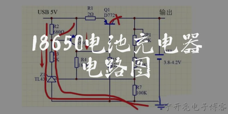
18650 Battery Charger Circuit Diagram:What is the basic circuit diagram of an 18650 battery charger?
Q: What is the basic circuit diagram of an 18650 battery charger?
A: A basic 18650 battery charger circuit diagram typically consists of a constant current/constant voltage (CC/CV) charging IC, a voltage regulator, and a battery holder. The most common design uses the TP4056 IC, which is a complete single-cell lithium-ion battery charger with a built-in CC/CV profile. In the diagram, the input power (usually 5V from USB) connects to the VCC and GND pins of the TP4056. A charge current is programmed by a resistor on the PROG pin; for 1A charging, a 1.2kΩ resistor is used. The BAT+ and BAT- terminals connect to the 18650 battery holder. The circuit also includes two LEDs: one for charging status and one for full charge, connected to the CHRG and STDBY pins through appropriate resistors. For safety, a protection circuit (e.g., DW01A with dual MOSFETs) is often added in series with the battery to prevent overcharge, over-discharge, and short circuits. The diagram should also show a 10µF input capacitor and a 10µF output capacitor to stabilize voltage. This minimal setup provides a reliable and safe way to charge 18650 cells.
Q: How do you connect multiple 18650 batteries in a charger circuit diagram?
A: When designing a circuit diagram for charging multiple 18650 batteries, you have two main options: parallel or series configurations. For parallel charging, connect all battery positive terminals together and all negative terminals together. This allows the use of a single-cell charger IC like the TP4056, but the charging current must be increased proportionally to the number of cells. For example, three parallel cells would require a 3A charge current, which may exceed the TP4056's 1A limit, so a higher-power charger IC like the BQ24195 or a dedicated multi-cell charger is needed. The circuit diagram should include individual protection circuits for each cell or a common protection board that can handle the total current. For series charging, cells are connected positive-to-negative, and a balance charger circuit is essential to ensure each cell charges equally. This requires a multi-cell charger IC such as the BQ25887 or a specialized balancing charger, which monitors each cell's voltage and adjusts charging accordingly. In the diagram, each cell's positive and negative terminals must be connected to the charger's corresponding sense and balance pins. Always include temperature sensing (NTC thermistor) and fuse protection in the diagram for safety.
Q: What safety features should be included in an 18650 charger circuit diagram?
A: A safe 18650 charger circuit diagram must incorporate several critical protection features. First, overcharge protection prevents the battery from exceeding 4.2V, typically implemented by the charger IC's voltage regulation loop or a dedicated protection IC like the DW01A. Second, over-discharge protection cuts off the load when voltage drops below 2.5V, avoiding cell damage; this is done via a MOSFET controlled by the protection IC. Third, overcurrent and short-circuit protection monitor the current through a sense resistor or the MOSFET's on-resistance. Fourth, temperature monitoring using an NTC thermistor connected to the charger IC's TEMP pin ensures charging stops if the battery overheats (above 45°C) or is too cold (below 0°C). Fifth, reverse polarity protection prevents damage if the battery is inserted incorrectly, often using a diode or P-channel MOSFET. Sixth, a charge status indicator (LEDs) helps users know the charging state. Finally, the circuit should include input fuse and transient voltage suppression to protect against power surges. All these features should be clearly labeled in the circuit diagram, and a proper PCB layout with adequate trace widths for current handling is essential. Always follow the manufacturer's datasheet recommendations for component values and placement.
Words of experience
Common scenarios of "18650 Battery Charger Circuit Diagram"
【Alex (Electronics Enthusiast)】 Hey Jamie, I'm trying to build a charger for my 18650 batteries. Can you help me understand the circuit diagram?
【Jamie (Electrical Engineer)】 Sure, Alex! I can walk you through it. First, do you have a specific charger IC in mind, like the TP4056?
【Alex (Electronics Enthusiast)】 Yes, I've heard about the TP4056. I want to design a circuit around it. What are the key components?
【Jamie (Electrical Engineer)】 Great choice! The TP4056 is a popular linear charger IC for 18650 cells. You'll need the IC itself, a few resistors, capacitors, and an LED for status indication.
【Alex (Electronics Enthusiast)】 Can you explain the pinout of the TP4056 and how to connect it?
【Jamie (Electrical Engineer)】 The TP4056 has 8 pins: TEMP, PROG, GND, VCC, BAT, STDBY, CHRG, and CE. VCC is the input voltage (4.5-5.5V), BAT connects to the battery positive, GND is ground, PROG sets the charge current with a resistor, CHRG and STDBY are LED outputs, TEMP is for temperature sensing, and CE is chip enable.
【Alex (Electronics Enthusiast)】 How do I set the charge current? I want to charge at 1A.
【Jamie (Electrical Engineer)】 The charge current is set by the resistor on the PROG pin. The formula is I = 1200 / R_PROG, where I is in amps and R in ohms. For 1A, R_PROG = 1200 / 1 = 1200 ohms. So use a 1.2k resistor.
【Alex (Electronics Enthusiast)】 Got it. What about the capacitors? I see some in typical schematics.
【Jamie (Electrical Engineer)】 Yes, you need input and output capacitors. A 10µF capacitor between VCC and GND for input filtering, and a 10µF between BAT and GND for output stability. Also, a small 0.1µF ceramic capacitor near VCC for noise.
【Alex (Electronics Enthusiast)】 And the LEDs? How do I connect them?
【Jamie (Electrical Engineer)】 Connect an LED from CHRG pin to VCC through a resistor (e.g., 1k) for charging indication, and another from STDBY to VCC through a resistor for standby/charge complete. The pins are open-drain, so they sink current when active.
【Alex (Electronics Enthusiast)】 What about the TEMP pin? Do I need to use it?
【Jamie (Electrical Engineer)】 If you don't use temperature sensing, connect TEMP to GND to disable it. If you want, you can connect a 10k NTC thermistor between TEMP and GND, and another resistor to VCC to form a voltage divider. But for simplicity, just ground it.
【Alex (Electronics Enthusiast)】 Okay, I'll ground TEMP. What about the CE pin?
【Jamie (Electrical Engineer)】 CE is active high. Connect it to VCC to enable the charger. You can also control it with a microcontroller if you want.
【Alex (Electronics Enthusiast)】 Now, I also want to add a protection circuit for over-discharge and over-current. Any suggestions?
【Jamie (Electrical Engineer)】 You can add a separate protection IC like the DW01A with dual MOSFETs, or use a protected 18650 cell. The TP4056 only handles charging, not discharge protection.
【Alex (Electronics Enthusiast)】 Thanks! I think I have a clear picture now. I'll draw the schematic and maybe simulate it.
【Jamie (Electrical Engineer)】 You're welcome! Double-check the connections, and remember to heat-sink the TP4056 if charging at 1A for long periods. Good luck with your build!