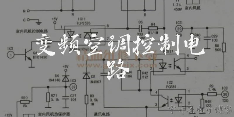
Integrated circuit design and manufacturing:What are the key steps involved in integrated circuit design and manufacturing?
Q: What are the key steps involved in integrated circuit design and manufacturing?
A: Integrated circuit design and manufacturing involve a series of highly complex steps. The process begins with design specification, where engineers define the chip's functionality, performance, and power requirements. Next, logic design and circuit design translate these specifications into schematics and gate-level netlists. Verification follows, using simulation and formal methods to ensure correctness. Physical design then places and routes components on the silicon die, optimizing for area, timing, and power. After tape-out, manufacturing begins with wafer fabrication. This includes crystal growth, wafer slicing, photolithography, etching, doping, and deposition to create transistors and interconnects layer by layer. Each layer requires precise masks and lithographic steps. Once wafers are fabricated, they undergo testing and dicing into individual chips. Packaging and final testing ensure the IC meets specifications. Advanced nodes like 5nm and 3nm demand extreme ultraviolet lithography and complex multi-patterning. Throughout, design for manufacturability and yield optimization are critical. The entire cycle can take months and involves collaboration between design houses, foundries, and equipment vendors.
Q: How do design and manufacturing interact in the semiconductor industry?
A: Design and manufacturing in the semiconductor industry are tightly coupled through a feedback loop known as design-technology co-optimization (DTCO). Designers must consider manufacturing constraints early, such as lithography limitations, process variation, and yield impact. For example, layout patterns that are difficult to print can cause defects, so design rules and recommended rules are provided by foundries. Conversely, manufacturing advances, like new transistor architectures (FinFET, GAA) or materials, enable new design possibilities. The interaction also extends to test structures and yield analysis: data from manufacturing feeds back to design to improve future revisions. In advanced nodes, this collaboration is essential because pushing performance and density requires simultaneous innovation in both domains. Electronic design automation (EDA) tools bridge the gap, offering features like parasitic extraction, timing analysis, and physical verification that align with process design kits (PDKs). Without this tight integration, achieving high yield and performance would be impossible. Thus, design and manufacturing are not sequential but iterative, driving the semiconductor roadmap forward.
Q: What are the major challenges in integrated circuit design and manufacturing today?
A: Integrated circuit design and manufacturing face several major challenges. First, scaling has slowed due to physical limits: as transistors approach atomic dimensions, quantum tunneling and leakage current become severe. Second, manufacturing costs have skyrocketed—a single advanced node fab can cost over $20 billion, and mask sets for 5nm can exceed $10 million. Third, design complexity is exploding: modern systems-on-chip (SoCs) contain billions of transistors, making verification and timing closure extremely difficult. Fourth, power density and thermal management are critical, especially for high-performance computing and mobile devices. Fifth, yield loss from process variations and defects remains a persistent issue, requiring extensive testing and redundancy. Sixth, the talent gap: there is a shortage of skilled engineers in both design and fabrication. Seventh, geopolitical factors and supply chain disruptions affect access to tools, materials, and foundries. Finally, emerging technologies like chiplets and 3D integration add new design and manufacturing hurdles. Addressing these challenges requires innovation in materials, architectures, EDA tools, and collaborative ecosystems.
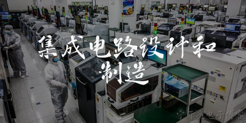
Dialogue about
Common scenarios of "Integrated circuit design and manufacturing"
【Interviewer】 Welcome to Tech Frontiers. Today we're exploring the fascinating world of integrated circuit design and manufacturing. I'm joined by Dr. Elena Chen, a senior IC designer, and Mark Rodriguez, a process engineer at a leading foundry. Welcome to both of you.
【Dr. Elena Chen】 Thanks for having me. It's great to discuss this topic, which is the backbone of modern electronics.
【Mark Rodriguez】 Happy to be here. I'm excited to share insights from the manufacturing side.
【Interviewer】 Let's start with the basics. Elena, what exactly is integrated circuit design?
【Dr. Elena Chen】 IC design is the process of creating the blueprint for a chip. It involves specifying the functionality, designing the circuit schematic, and then translating that into a physical layout that can be manufactured. We use electronic design automation (EDA) tools to simulate and verify the design before it goes to fabrication.
【Interviewer】 And Mark, what does manufacturing entail?
【Mark Rodriguez】 Manufacturing, or fabrication, is where the design becomes a physical silicon chip. We start with a silicon wafer and use a series of steps like photolithography, etching, deposition, and doping to build up the layers of transistors and interconnects. It's a highly complex process with hundreds of steps, often taking months from start to finish.
【Interviewer】 How do design and manufacturing interact? Elena, from your perspective?
【Dr. Elena Chen】 Designers must be aware of manufacturing capabilities and constraints. For example, the minimum feature size that can be reliably printed on a wafer affects how densely we can pack transistors. We work closely with foundries to understand their design rules, which ensure the design can be manufactured with acceptable yield.
【Mark Rodriguez】 Absolutely. And as process nodes shrink, the interactions become more critical. At advanced nodes like 5nm or 3nm, design and process co-optimization is essential. We often provide feedback to designers on how certain layout choices might impact yield or performance.
【Interviewer】 What are some of the biggest challenges in IC design today?
【Dr. Elena Chen】 One major challenge is power consumption. As we pack more transistors, managing heat and power becomes critical. Also, design complexity is skyrocketing; a modern system-on-chip can have billions of transistors, and verifying that it works correctly requires enormous computational resources.
【Interviewer】 And from the manufacturing side, Mark?
【Mark Rodriguez】 The cost and complexity of advancing to smaller nodes are huge. Each new node requires billions of dollars in R&D and new equipment, like extreme ultraviolet (EUV) lithography. Also, yield ramp is challenging; getting a new process to produce chips with high yield takes time and constant tweaking.
【Interviewer】 Elena, how do designers address yield issues?
【Dr. Elena Chen】 We use design for manufacturability (DFM) techniques. This includes adding redundant vias, optimizing layout for better lithography, and incorporating error correction codes. We also work with foundries to run test chips and use statistical analysis to predict yield and identify marginal designs.
【Interviewer】 Mark, can you explain a bit about the process nodes and why they matter?
【Mark Rodriguez】 Process nodes, like 7nm, 5nm, etc., refer to the technology generation and roughly the size of the smallest features. Smaller nodes allow more transistors per area, leading to faster, more power-efficient chips. But they also bring quantum tunneling effects and other challenges. The naming is somewhat arbitrary now; it's more about marketing and technology generation than actual dimensions.
【Interviewer】 What about the future? Elena, what trends do you see in IC design?
【Dr. Elena Chen】 We're seeing a shift towards domain-specific architectures, like AI accelerators, and chiplets, where multiple smaller dies are integrated in a package. Also, 3D integration is gaining traction, stacking dies vertically to improve performance and reduce footprint.
【Mark Rodriguez】 And manufacturing is evolving to support these trends. We're developing advanced packaging technologies like through-silicon vias (TSVs) and hybrid bonding to enable 3D stacking. Also, we're exploring new materials beyond silicon, like gallium nitride for power electronics.
【Interviewer】 Thank you both for a fascinating discussion. It's clear that IC design and manufacturing are deeply intertwined and constantly pushing the boundaries of technology.
【Dr. Elena Chen】 Thank you. It's an exciting field to be in.
【Mark Rodriguez】 Thanks for having us. The future of chips is bright!